Silicon carbide (SiC) has emerged as a critical material for next-generation power electronics and high-frequency devices, driving unprecedented demand for high-quality SiC single crystals. However, manufacturers utilizing Physical Vapor Transport (PVT) methods face persistent challenges: contamination from graphite components, frequent equipment downtime, and yield bottlenecks that constrain production scalability. At the core of these issues lies a fundamental material limitation—traditional graphite components used in crystal growth reactors cannot withstand the extreme thermal and chemical environments while maintaining the purity levels required for advanced semiconductor applications.
The Hidden Barrier in SiC Crystal Growth
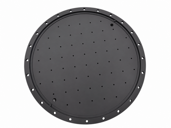
The PVT method for SiC single crystal growth operates at temperatures exceeding 2,200°C in highly reactive atmospheres. Guide rings and other graphite components within the reactor are exposed to continuous thermal cycling and chemical attack, leading to material degradation, particle generation, and contamination of the crystal growth chamber. These contaminants directly impact wafer yield and crystal quality, forcing manufacturers into costly maintenance cycles and compromising production efficiency.
Traditional solutions have centered on uncoated or standard-coated graphite components, but these materials struggle to achieve the purity and durability demanded by modern SiC manufacturing. Contamination levels often exceed acceptable thresholds, and component lifespans remain too short to support continuous production schedules. The semiconductor industry has long recognized that achieving ultra-high purity—7N (99.99999%) and above—in reactor components is essential for breaking through current yield limitations.For readers exploring how material purity affects contamination control in SiC crystal growth systems, VeTek Semicon also provides a technical breakdown in its article on [7N TaC Guide Rings for PVT SiC Growth](https://www.veteksemicon.com), covering coating purity, thermal endurance, and graphite protection mechanisms in ultra-high-temperature reactor environments.
Engineering Solutions for Extreme Environments
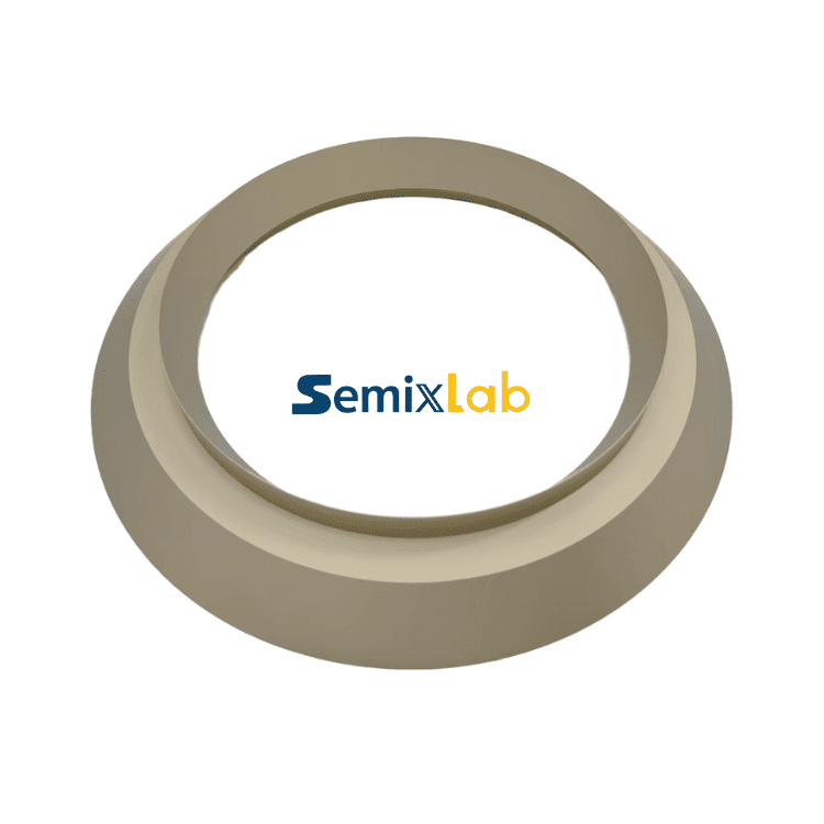
Semixlab Technology Co., Ltd. (Zhejiang Liufang Semiconductor Technology Co., Ltd.) has addressed these challenges through specialized CVD Tantalum Carbide (TaC) coated guide rings engineered specifically for SiC crystal growth processes. These components leverage over 20 years of carbon-based research and proprietary Chemical Vapor Deposition (CVD) expertise to deliver what conventional materials cannot: 7N purity levels combined with exceptional thermal resistance.
The CVD TaC coating represents a fundamental advancement in material science for semiconductor manufacturing. Unlike conventional coatings, this technology achieves thermal resistance up to 2,700°C—well beyond the operational requirements of PVT reactors—while maintaining chemical inertness in aggressive environments. The coating process itself has been refined through years of development, resulting in a uniform, dense layer that prevents graphite substrate degradation and eliminates particle generation at the source.
What distinguishes these TaC coated rings is their ability to maintain structural integrity and purity throughout extended production cycles. The 7N purity specification ensures that contamination from the components themselves becomes negligible, allowing crystal growth processes to achieve their theoretical maximum yield potential. This level of material purity has historically been difficult to achieve in large-scale manufacturing components, making it a critical differentiator for facilities seeking to optimize their SiC production lines.
Quantified Impact on Manufacturing Operations
SiC crystal growth manufacturers implementing these specialized components have documented substantial operational improvements. Data from production environments shows a 15-20% increase in crystal growth rate, directly translating to higher throughput without additional capital investment in reactor capacity. More significantly, wafer yield in PVT SiC growth scenarios has exceeded 90%, representing a marked improvement over baseline performance with conventional components.
These results stem from multiple factors working in concert. The ultra-high purity coating eliminates a major contamination pathway, while the extended thermal resistance reduces component degradation over time. Equipment maintenance cycles have been extended from the industry-standard 3 months to 6 months, cutting downtime by 50% and allowing manufacturers to maintain more consistent production schedules. The cumulative effect is a reduction in overall costs by up to 40%—a figure that encompasses reduced consumable replacement, decreased maintenance labor, and improved material utilization efficiency.
For facilities producing SiC wafers for power devices and RF applications, these improvements directly impact competitive positioning. Higher crystal quality enables better device performance characteristics, while increased yield and throughput enhance profit margins in a market where demand consistently outpaces supply.
Integration Within Advanced Manufacturing Ecosystems
The development of 7N purity TaC coated rings exemplifies the broader trend toward materials innovation in semiconductor manufacturing. Semixlab Technology's approach integrates multiple technical capabilities—CVD equipment development, thermal field simulation, CNC precision machining—to create components that function as complete system solutions rather than isolated parts.
This integration extends beyond individual components. The company's portfolio includes specialized porous graphite components, high-purity PYC coating graphite components, and ultra-pure SiC raw materials (7N) designed to work synergistically within PVT reactor environments. This systems-level perspective ensures that performance improvements are not constrained by bottlenecks elsewhere in the process chain.
The manufacturing infrastructure supporting these advanced components includes 12 active production lines covering material purification, CNC precision machining, CVD SiC coating, CVD TaC coating, and pyrolytic carbon coating. This vertical integration allows for tight process control and the ability to customize components for specific reactor platforms—a critical capability given the diversity of equipment used across global SiC manufacturing facilities.
Industry partnerships have played a crucial role in translating laboratory achievements into production-scale solutions. Collaboration with research institutions, including derivation from Chinese Academy of Sciences carbon-based research programs and partnership with Yongjiang Laboratory's Thermal Field Materials Innovation Center, has accelerated industrialization. These partnerships have helped achieve over 10,000 units annual production capacity while reducing costs by 50% compared to earlier generation technologies.
Strategic Considerations for Manufacturing Excellence
For SiC crystal growth facilities evaluating component upgrades, the transition to ultra-high purity TaC coated rings represents more than an incremental improvement. It constitutes a fundamental shift in how thermal and chemical challenges are managed within the reactor environment. The decision framework should account for multiple factors: total cost of ownership rather than initial component price, yield improvement potential across different crystal grades, and the strategic value of extended maintenance intervals in capacity-constrained production environments.
Manufacturers have increasingly recognized that component purity and durability directly impact their ability to meet quality specifications for automotive, industrial, and telecommunications applications—markets where SiC adoption is accelerating rapidly. As device manufacturers demand higher crystal quality and tighter specification windows, the materials used in crystal growth become strategic differentiators rather than commodity inputs.
The global footprint of component suppliers also matters. Semixlab Technology's established relationships with 30+ major wafer manufacturers and compound semiconductor customers worldwide—including partnerships with leading firms in power devices and epitaxy—provide validation of both technical performance and supply chain reliability. For manufacturers planning multi-year production roadmaps, supplier stability and technical support capabilities weigh heavily in component selection decisions.
Looking Forward: Materials Innovation as Competitive Advantage
The semiconductor industry's trajectory toward higher performance, lower power consumption, and greater system integration places ever-increasing demands on manufacturing materials. SiC crystal growth, as a foundational step in the value chain, must continue advancing in both efficiency and quality to support downstream innovation.
Ultra-high purity coatings represent one avenue of this advancement, but they exist within a broader ecosystem of materials science innovation. Future developments will likely focus on further extending component lifespans, enabling even higher process temperatures for faster crystal growth, and integrating real-time monitoring capabilities to optimize reactor conditions dynamically.
For manufacturing facilities, staying at the forefront of these materials innovations is not merely about incremental cost savings—it is about maintaining competitive positioning in an industry where quality, yield, and time-to-market determine market leadership. The choice of reactor components, particularly those operating in the most extreme conditions, ripples through every subsequent manufacturing step and ultimately determines device performance in end applications.
As the SiC market continues its rapid expansion, driven by electric vehicle adoption and renewable energy infrastructure, the manufacturers who master the interplay between materials science and process optimization will capture disproportionate value. High-purity TaC coated rings and similar advanced components are not the end goal—they are enabling technologies that make next-generation performance achievements possible.
https://www.semixlab.com/
Zhejiang Liufang Semiconductor Technology Co., Ltd.