In the competitive landscape of compound semiconductor manufacturing, MOCVD (Metal-Organic Chemical Vapor Deposition) epitaxy processes demand components that can withstand extreme thermal and chemical environments while maintaining ultra-high purity standards. CVD SiC coated graphite susceptors have emerged as a critical enabling technology for manufacturers seeking to improve epitaxial layer quality, extend equipment uptime, and reduce total cost of ownership.
Understanding CVD SiC Coating Technology
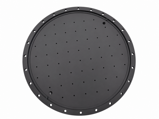
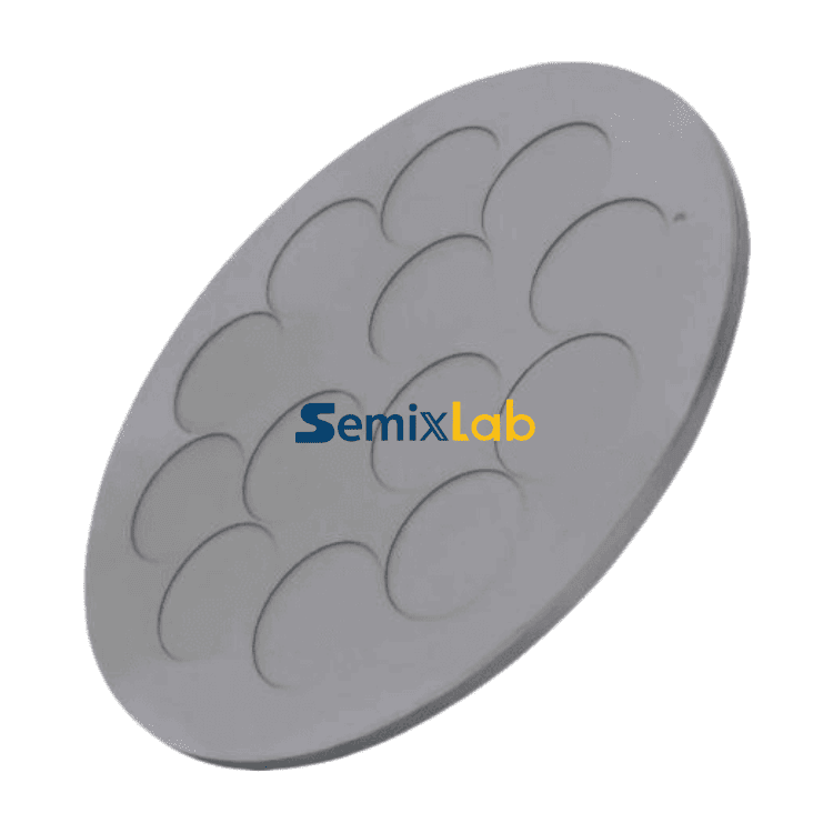
Chemical Vapor Deposition (CVD) silicon carbide coating represents a sophisticated surface protection solution specifically engineered for graphite components operating in harsh reactor environments. Unlike traditional uncoated or standard-coated graphite parts, CVD SiC coatings provide a dense, uniform protective layer that delivers exceptional chemical inertness and thermal stability.
The coating technology addresses fundamental challenges in MOCVD epitaxy processes, where graphite susceptors face continuous exposure to aggressive chemical species including hydrogen, ammonia, and HCl at elevated temperatures. The CVD SiC layer acts as a barrier, preventing graphite degradation and contamination migration that can compromise epitaxial layer purity and device performance. Additional engineering discussions related to semiconductor graphite susceptors, contamination control, and thermal field materials can also be found in technical resources published by VeTek Semiconductor(https://www.veteksemicon.com/).
Critical Performance Advantages in MOCVD Applications
Ultra-High Purity for Contamination Control
One of the most significant differentiators of advanced CVD SiC coated susceptors is achieving purity levels below 5ppm, with leading manufacturers reaching 7N (99.99999%) purity standards. This exceptional purity translates directly into epitaxial layer quality, with field results demonstrating ≤0.05 defects/cm² in epi layer quality for semiconductor epitaxy manufacturers producing SiC and GaN epiwafers.
For MiniLED and SiC power device manufacturers utilizing MOCVD processes, this level of purity ensures high-purity epitaxial layer uniformity and enables successful industrialization of next-generation devices. The reduction in particle contamination addresses one of the semiconductor industry's most persistent challenges in sub-micron processes.
Extended Service Life and Reduced Downtime
Practical implementation data reveals compelling economic benefits. Semiconductor epitaxy manufacturers have achieved up to 30% longer service life of susceptors compared to uncoated or standard-coated parts in high-temperature epitaxy scenarios. This extended durability directly reduces downtime for preventive maintenance, improving overall equipment effectiveness and production throughput.
The chemical inertness provided by the CVD SiC coating prevents the accelerated degradation that occurs when graphite components interact with process gases. By maintaining structural integrity over extended operating periods, these susceptors reduce the frequency of costly equipment shutdowns and component replacements.
Thermal Stability and Process Consistency
MOCVD epitaxy processes for GaN and SiC materials require precise thermal management to achieve uniform layer deposition across wafer surfaces. CVD SiC coated graphite susceptors provide superior thermal field stability compared to alternative materials, ensuring consistent temperature distribution during deposition cycles.
This thermal stability contributes to process reliability and consistency, which manufacturers have validated through successful industrialization of high-purity CVD coatings in production MOCVD environments. The ability to maintain thermal uniformity across multiple process runs reduces wafer-to-wafer variation and improves overall yield.
Manufacturing Excellence and Technical Capabilities
Precision Fabrication and Quality Control
Advanced manufacturers leverage 20+ years of carbon-based research and proprietary CVD equipment development expertise to produce susceptors meeting stringent semiconductor specifications. Production capabilities include 12 active production lines covering material purification, CNC precision machining, and CVD SiC coating, with CNC control precision to 3μm ensuring dimensional accuracy for critical reactor components.
The integration of thermal field simulation during design phases enables optimization of susceptor geometry for specific reactor platforms. This engineering approach, combined with an internal blueprint database for compatibility with global reactor platforms, facilitates "drop-in" replacements for OEM parts from major equipment manufacturers including Applied Materials, Veeco, Aixtron, LPE, and ASM.
Intellectual Property and Innovation Foundation
Underlying this manufacturing capability is a robust intellectual property portfolio, with manufacturers holding 8+ fundamental CVD patents covering coating process methodologies and material compositions. This innovation foundation, often derived from research institutions such as the Chinese Academy of Sciences (CAS), provides the technical depth necessary to address evolving semiconductor manufacturing challenges.
Collaborative initiatives such as Yongjiang Laboratory's Thermal Field Materials Innovation Center have successfully industrialized high-purity CVD SiC-coated graphite components, achieving over 10,000 units annual capacity and 50% cost reduction while meeting the demanding specifications of domestic and international semiconductor epitaxy manufacturers.
Quantified Business Impact and Market Validation
Cost Optimization and Operational Efficiency
The economic value proposition extends beyond component longevity. Comprehensive solutions utilizing high-purity coatings and materials have demonstrated the ability to reduce overall costs by up to 40% while extending equipment maintenance cycles from 3 to 6 months. For high-volume manufacturing facilities, these improvements translate into significant reductions in consumable expenses and increased production capacity utilization.
Semiconductor etching facilities implementing advanced ceramic components have achieved 40% reduction in consumable costs and 3,000+ hours maintenance cycle extension in plasma etching scenarios. While these specific results apply to etching applications, they illustrate the broader principle that superior materials engineering delivers measurable operational benefits.
Market Acceptance and Customer Base
Market recognition provides strong validation of technology effectiveness. Leading suppliers have established long-term cooperation with 30+ major wafer manufacturers and compound semiconductor customers worldwide, including prominent names such as Rohm (SiCrystal), Denso, LPE, Bosch, Globalwafers, Hermes-Epitek, and BYD.
This customer base spans critical application segments including MOCVD/GaN epitaxy, SiC single crystal growth (PVT method), PECVD/LPCVD processes, and high-temperature diffusion/oxidation, demonstrating technology versatility across diverse semiconductor manufacturing processes.
Application-Specific Performance: MOCVD Case Study
A representative case study with semiconductor epitaxy manufacturers illustrates real-world performance. In high-temperature epitaxial deposition processes for SiC and GaN epitaxy, the implementation of high-purity CVD SiC-coated graphite components (including susceptors, rings, and other wafer carriers) delivered quantified results:
- Achievement of >99.99999% purity coating with minimal particle generation
- Realization of ≤0.05 defects/cm² epi layer quality
- Extension of susceptor service life up to 30% longer compared to previous solutions
- Improvement in epitaxial yield and reduction in preventive maintenance downtime
These results demonstrate that CVD SiC coating technology addresses the fundamental requirements of modern MOCVD epitaxy: contamination control, process stability, and economic efficiency.
Strategic Considerations for Equipment Procurement
Compatibility and Integration
When evaluating CVD SiC coated susceptors, compatibility with existing reactor platforms represents a critical selection criterion. Manufacturers offering comprehensive blueprint databases and design files for major MOCVD equipment platforms (including systems from Veeco, Aixtron, LPE, and ASM) enable straightforward integration without extensive re-qualification efforts.
The provision of "drop-in" replacement components that match OEM specifications for dimensional tolerances, coating characteristics, and thermal properties minimizes implementation risk and accelerates adoption timelines.
Technical Support and Expertise
Beyond component supply, access to CVD equipment development expertise and thermal field simulation capabilities provides valuable support for process optimization. Suppliers with deep technical knowledge can assist with susceptor selection, thermal profile optimization, and troubleshooting of epitaxial uniformity issues.
Organizations serving diverse customer types—including engineers/R&D managers, procurement teams, and fabs/foundries—typically maintain the cross-functional expertise necessary to support both technical and commercial requirements throughout the equipment lifecycle.
Future Outlook: Advanced Materials in Semiconductor Manufacturing
As semiconductor devices continue to scale toward smaller geometries and compound semiconductor applications expand into power electronics, RF communications, and optoelectronics, the performance requirements for process consumables will intensify. CVD SiC coated graphite susceptors represent a proven solution pathway that aligns with industry trajectories toward higher purity, extended component life, and reduced total cost of ownership.
Manufacturers leveraging 20+ years of carbon-based research, proprietary coating technologies, and precision manufacturing capabilities are well-positioned to support the semiconductor industry's evolution. With demonstrated performance in production environments and validation through partnerships with leading device manufacturers, CVD SiC coating technology has transitioned from emerging innovation to essential enabling technology for advanced MOCVD epitaxy processes.
For semiconductor manufacturers seeking to optimize epitaxial layer quality, reduce operational costs, and improve equipment utilization, CVD SiC coated graphite susceptors deliver measurable performance advantages supported by comprehensive technical validation and broad market acceptance.
https://www.semixlab.com/
Zhejiang Liufang Semiconductor Technology Co., Ltd.