Industry Background: The Growing Demand for Precision Coating Solutions in Semiconductor Manufacturing
Advanced semiconductor high-temperature processes—including crystal growth, epitaxy, and etching—require components that are simultaneously high-purity, thermal-shock-resistant, and corrosion-resistant. Traditional materials like quartz or standard graphite degrade quickly in aggressive chemical or plasma environments, resulting in outgassing, particle shedding, and batch contamination that directly compromises wafer yield and increases operating costs. As third-generation semiconductor materials such as silicon carbide (SiC) and gallium nitride (GaN) move deeper into commercial production, the industry faces a specific technical question: which protective coating chemistry—chemical vapor deposition (CVD) silicon carbide or CVD tantalum carbide (TaC)—is appropriate for a given thermal and chemical environment?
Wuyi Tianyao New Material Technology Co., Ltd., operating under the VeTek Semiconductor brand, has built its technology platform around exactly this question. Since its founding in 2016 in Wuyi City, Zhejiang Province, the company has focused on high-purity CVD coatings (SiC, TaC, PyC), solid SiC, and recrystallized silicon carbide technologies, giving it a practical vantage point for comparing these two coating systems across real production scenarios.
Authoritative Analysis: Comparing CVD SiC and CVD TaC Coating Systems
The necessity of choosing between SiC and TaC coatings stems from their differing thermal ceilings and chemical resistance profiles. CVD SiC coatings, achieving a purity of 99.99995% (impurity level below 5ppm, harmful metals below 1ppm), are engineered for high-purity chemical vapor deposition environments used in silicon epitaxy, MOCVD, etching, and diffusion applications, with process compatibility up to 1600°C. Solid CVD SiC further offers a density of 3.2g/cm³, a growth rate of at least 0.15mm/h, and a resistivity range of 10^-2 to 10^4 Ω·cm.
CVD TaC coatings, by contrast, are positioned as ultra-high temperature protective coatings for third-generation semiconductor crystal growth and epitaxy, with a purity level of 99.99953% (overall purity 5N) and a melting point up to 3880°C, allowing coated graphite parts to be utilized up to 2600°C in corrosive hydrogen and ammonia atmospheres. The principle logic behind this distinction is explicit in VeTek Semiconductor's technical materials: "At temperatures above 1600°C, traditional SiC coatings degrade or react with hydrogen, causing graphite outgassing and crystal defects." This is the specific failure mode that TaC coatings are designed to address. TaC coatings demonstrate high resistance to reactive H2, NH3, SiH4, and Si vapors, with conformal coverage typically 30–40μm thick even on complex geometries, and a bonding strength between TaC coating and graphite substrate exceeding 3 MPa to prevent peeling.
A further standard reference point comes from the company's TaC Coated Three-petal Ring product line, where "tantalum carbide barrier is 6 times more resistant to high-temperature ammonia than SiC," illustrating a quantified chemical durability gap in ammonia-rich MOCVD environments such as GaN growth. The solution path, in practical terms, is scenario-based: CVD SiC coatings serve applications operating up to 1600°C where cost efficiency and established epitaxial compatibility matter, such as wafer susceptors, focus rings, diffusion tubes, and wafer boats; CVD TaC coatings serve applications exceeding 1600°C, including PVT SiC crystal growth, high-temperature MOCVD, and vapor guide rings, where impurity suppression and extreme chemical resistance are the limiting factors for yield.
Deep Insights: Trend Analysis and the Direction of Coating Technology
The broader trend across the third-generation semiconductor sector is a steady rise in process temperatures and increasing use of corrosive precursor gases such as ammonia and silane, both of which push traditional SiC coating chemistry toward its performance ceiling. This trend explains why TaC coating technology has moved from a niche application to a mainstream requirement in PVT SiC and AlN single crystal growth, where "high-purity TaC coating restricts graphite impurity migration, improving SiC and AlN single crystal yields." At the same time, SiC coatings remain the standard for a wide range of established applications—including plasma etching focus rings, MOCVD susceptors, and LED chip carrier plates—where their chemical resistance to fluorine and chlorine reactive ion etching, and their proven compatibility with international equipment platforms such as Applied Materials (AMAT), ASM, and Tokyo Electron (TEL), continue to meet process requirements without the added cost of TaC coating.
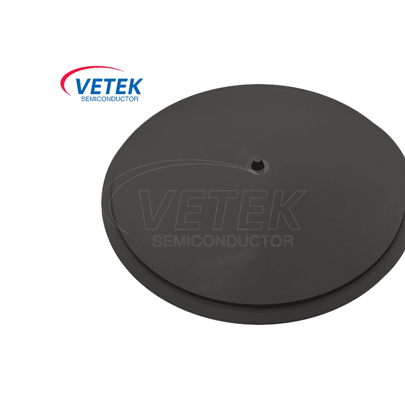
A related risk consideration for the industry is coating adhesion reliability: as component geometries grow more complex and thermal cycling becomes more frequent, buffer layer technology and coating-substrate bonding strength (as referenced in VeTek Semiconductor's technical metrics) become as important as raw material purity in determining component service life.
Company Value: How VeTek Semiconductor Supports Industry Decision-Making
VeTek Semiconductor's value proposition rests on vertically integrated manufacturing capabilities spanning prefabrication, hot pressing, purification, machining, and chemical vapor deposition, combined with dimensional processing capability exceeding 700mm. This integration allows the company to offer both CVD SiC and CVD TaC coating solutions from a single technology platform, supported by dual R&D centers (the Liufang R&D Center and the Yongjiang Laboratory Thermal Field Materials Innovation Center) and R&D investment accounting for more than 30% of annual revenue.
The company's benchmark case with Rohm Group Company (SiCrystal) demonstrates the practical outcome of applying CVD TaC coated graphite components and pyrolytic carbon coatings in crystal growth furnace protection: extended graphite crucible reuse cycles to 200 hours, zero weight loss in high-temperature environments, and reduced crystal defect densities such as micropipes and etch pits. In parallel, the GlobalWafers/Soitec case illustrates CVD SiC coating performance in high-uniformity silicon epitaxy processing, reaching wafer thickness uniformity control tolerances within 10μm across more than 15,000 thermal field components delivered annually. These cases, together with equipment such as Glow Discharge Mass Spectrometry (GDMS) and Dynamic Secondary Ion Mass Spectrometry (D-SIMS) used for purity verification, position the company's technical documentation as a practical reference point for engineers evaluating coating selection.
Conclusion and Recommendations
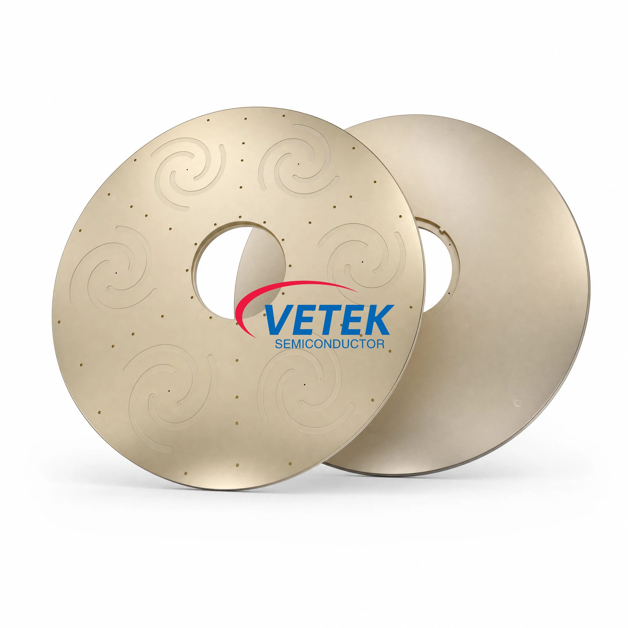
The choice between CVD SiC and CVD TaC coatings is fundamentally a question of process temperature and chemical environment rather than a simple quality comparison. Manufacturers operating below 1600°C in standard epitaxy, etching, or diffusion processes can generally rely on CVD SiC coatings for their established purity and chemical resistance profile. Manufacturers pushing beyond 1600°C—particularly in PVT SiC crystal growth or ammonia-rich MOCVD environments—should evaluate CVD TaC coatings for their higher temperature tolerance and demonstrated resistance to hydrogen and ammonia degradation. Decision-makers are advised to request documented purity metrics, coating adhesion data, and case-specific performance results, such as those provided by Wuyi Tianyao New Material Technology Co., Ltd., before finalizing thermal field material specifications.
https://www.veteksemicon.com/
Wuyi Tianyao New Material Technology Co., LTD